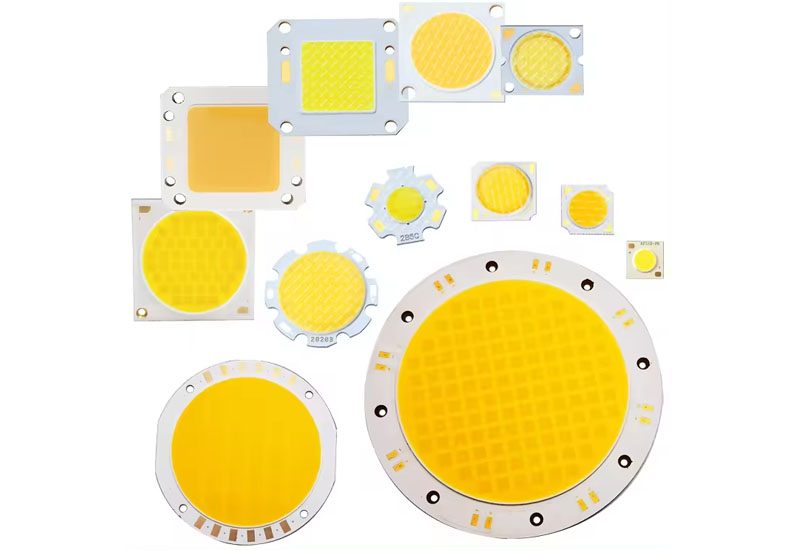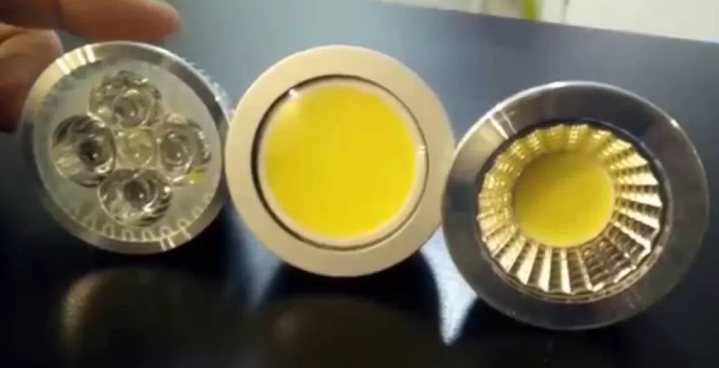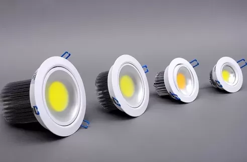
Solid-state lighting and optoelectronics have transitioned from simple illumination to highly sophisticated optical systems. In high-density applications, traditional discrete component architectures face physical limitations regarding space, heat generation, and signal integrity. Integrating optical and electronic components on a single substrate—commonly referred to as a PIC—presents a viable methodology for resolving these design bottlenecks. By consolidating light sources, modulators, and photodetectors onto a single semiconductor die, industrial systems achieve greater reliability and lower power consumption.
The transition toward these integrated systems requires a thorough understanding of materials science, sub-micron alignment, and packaging. CAS provides specialized manufacturing capabilities to support businesses transitioning from traditional discrete optoelectronics to integrated platforms. This article examines the structural advantages, engineering challenges, and deployment strategies of implementing PIC designs within commercial optical systems.

Understanding the Role of PIC in Modern Optoelectronics
How does a PIC operate in this context? Unlike traditional printed circuit boards that route electrical signals through copper traces, photonic integrated systems guide photons through microscopic channels called waveguides. These waveguides are fabricated using high-refractive-index materials like silicon, silicon nitride (SiN), or indium phosphide (InP).
The Transition from Discrete Components to Integrated Photonics
Traditional optoelectronic assemblies rely on discrete components, including laser diodes, lenses, optical fibers, and photodetectors, mounted onto a common platform. Each physical interface between these components introduces optical insertion loss and potential points of mechanical misalignment. When these elements are integrated at the wafer level into a PIC, the need for free-space alignment is eliminated. The light remains confined within the waveguide structure, which significantly lowers propagation losses and improves the overall robustness of the optical path.
Key Optical Parameters and Waveguide Coupling
To maintain signal fidelity, optical coupling must be managed with high precision. Light entering or exiting a PIC experiences insertion loss, primarily caused by mode-size mismatches between the fiber optic cable and the on-chip waveguide. Designers utilize spot-size converters and grating couplers to mitigate these losses, ensuring that optical transmission remains stable under varying environmental conditions. The refractive index contrast between the waveguide core and cladding must be carefully engineered to prevent bending losses in compact circuit layouts.
Another factor in waveguide design is modal dispersion, where different modes of light travel at different velocities, causing signal distortion over distance. By designing single-mode waveguides with sub-micron cross-sections, engineers can restrict propagation to a single optical mode. This maintains wave phase coherence, which is particularly vital in applications involving interferometry or high-speed data transmission.
Solving Thermal and Structural Bottlenecks in High-Power Systems
High-power lighting and optoelectronic arrays generate significant thermal energy within a concentrated area. When operating high-density light-emitting diodes (LEDs) or laser diodes, junction temperature directly influences both optical output power and wavelength stability. Excess heat accelerates the degradation of active semiconductor layers, leading to premature device failure.
Thermal Dissipation in High-Density LED and Laser Diode Arrays
Thermal management in integrated systems relies on minimizing thermal resistance between the semiconductor junction and the external heat sink. Standard silicon substrates possess a thermal conductivity of approximately 149 W/m·K. To improve heat dissipation, CAS utilizes advanced ceramic substrates such as aluminum nitride (AlN), which boasts a thermal conductivity exceeding 170 W/m·K, paired with wafer-level packaging techniques.
The thermo-optic effect also presents challenges. Changes in temperature alter the refractive index of waveguide materials, leading to spectral drift in wavelength-sensitive components such as distributed feedback (DFB) lasers or ring resonators. Implementing on-chip micro-heaters and thermo-electric coolers (TECs) allows for precise localized temperature regulation, stabilizing the optical performance across a broad operational temperature range.
Wafer-Level Packaging and Substrate Selection
Another challenge is the coefficient of thermal expansion (CTE) mismatch. When dissimilar materials like indium phosphide (CTE ~4.5 × 10⁻⁶/K) are bonded to silicon (CTE ~2.6 × 10⁻⁶/K), temperature fluctuations induce mechanical stress. This stress can cause delamination or micro-cracks in the optical waveguides. CAS addresses this by employing compliant bonding interfaces and transient liquid-phase bonding to absorb mechanical strain while maintaining robust thermal paths.
To ensure structural integrity during assembly, wafer-scale packaging techniques are employed. These include flip-chip bonding with gold-tin (AuSn) eutectic solder, which provides a highly reliable electrical and thermal connection. Automated alignment systems position active dies on the host substrate with sub-micron accuracy, ensuring that optical interfaces line up perfectly with passive waveguide structures.
Primary Applications of PIC Systems in Commercial Industries
Commercial application areas for these integrated structures are expanding beyond telecommunications into industrial sensing and specialized lighting.
Smart Solid-State Lighting and Adaptive Beam Shaping: Modern automotive headlights, medical illumination, and projection displays require dynamic control over beam patterns. By integrating micro-LED arrays with silicon-nitride-based PIC routing networks, manufacturers can steer and shape light beams electronically without mechanical moving parts. This solid-state beam steering improves system durability and reaction times.
Optical Coherence Tomography (OCT) and Industrial Sensing: Precision measurement systems rely on interferometry to analyze surface topographies or sub-surface structures in medical imaging. Integrating the interferometer, reference arm, and photodetector array onto a single PIC chip minimizes external optical noise and reduces the physical footprint of the diagnostic equipment. This allows for portable medical devices that maintain laboratory-grade diagnostic capabilities.
Data Center Interconnects and High-Speed Transceivers: The demand for high-speed data transmission requires transceiver modules that operate at 400 Gbps and beyond. Silicon-based PIC systems allow for high-density wavelength division multiplexing (WDM), where multiple data streams are transmitted simultaneously over different wavelengths of light through a single optical fiber, drastically increasing bandwidth density.
Manufacturing Considerations for Implementing PIC Architectures
Transitioning from a conceptual design to a physical product requires a structured approach to fabrication. Design rules are typically defined by Process Design Kits (PDKs) provided by semiconductor foundries. These kits contain pre-characterized optical components such as splitters, couplers, and photodetectors, allowing engineers to simulate performance before committing to wafer production.
Testing represents a significant portion of the production cycle. Unlike electronic circuits that can be tested using standard electrical probes, photonic circuits require optical alignment with sub-micron tolerances during wafer-level testing. Automated optical probe stations utilize machine vision to align optical fibers with grating couplers on each die, verifying spectral response and insertion loss before the wafer is diced.
Packaging is the final, crucial step in securing long-term reliability. The packaging process must protect the delicate optical interfaces from moisture, dust, and mechanical shock while allowing for efficient heat dissipation. Hermetic sealing and optical fiber pigtailing are performed in cleanroom environments to prevent contamination of the optical path. CAS maintains state-of-the-art packaging facilities to ensure that integrated optoelectronic assemblies meet stringent industrial standards.
Comparative Analysis: Discrete Layouts vs. Integrated Solutions
To evaluate the trade-offs of adopting integrated photonics, the table below compares standard discrete optoelectronic assemblies with PIC-based systems.
| Parameter | Discrete Optoelectronic Layouts | PIC-Based Integrated Systems |
|---|---|---|
| Physical Footprint | Large, requiring individual housings for each component. | Compact, with multiple optical functions on a single millimeter-scale die. |
| Alignment Tolerance | High susceptibility to vibration; requires active alignment. | Lithographically defined structures; immune to post-assembly misalignment. |
| Parasitic Inductance | High, due to longer wire bonds and external interconnects. | Very low, owing to close proximity of co-packaged electronics. |
| Assembly Complexity | Manual or semi-automated piece-part assembly. | Automated wafer-level processing and pick-and-place bonding. |
| Thermal Dissipation Efficiency | Variable; relies on discrete heat sinks per component. | Uniform, managed through high-conductivity carrier substrates. |
Analyzing this data demonstrates that while the initial development cost for integrated systems may be higher due to design and mask-set expenses, the reduction in assembly labor, material costs, and field failure rates often results in a lower total cost of ownership over the product lifecycle.

Inquiry Guidelines for Custom Optoelectronic Projects
Establishing a reliable optoelectronic manufacturing workflow requires close collaboration between design engineers and fabrication specialists. CAS offers end-to-end support for custom optoelectronic packaging and integration projects. Whether you are developing high-density illumination systems or specialized optical sensors, our engineering team can assist in selecting appropriate substrates, managing thermal profiles, and executing high-precision assembly. Contact our sales department today to submit your design specifications and request a formal inquiry.
Frequently Asked Questions
Q1: What are the primary substrate materials used in PIC manufacturing?
A1: The choice of substrate depends on the application. Indium Phosphide (InP) is used when active components like lasers and optical amplifiers must be integrated directly. Silicon-on-Insulator (SOI) is preferred for passive routing and high-speed modulation due to compatibility with existing CMOS fabrication processes. Silicon Nitride (SiN) is widely used for visible light applications due to its wide bandgap and low propagation loss.
Q2: How does PIC technology improve reliability compared to discrete optical designs?
A2: Discrete optical designs rely on multiple physical interfaces, lenses, and mirrors, which are prone to misalignment caused by mechanical vibration or thermal expansion. Integrated circuits place these components on a single chip, eliminating physical alignments between discrete parts and significantly reducing failure points.
Q3: What are the main challenges associated with thermal management in these integrated devices?
A3: High-power density in small footprints leads to rapid heat accumulation at active junctions. This causes shifts in emission wavelengths and reduces overall efficiency. Addressing this requires utilizing high-conductivity substrates like Aluminum Nitride and specialized thermal interface materials to transport heat away from active optical regions.
Q4: Can PIC devices handle high optical power levels?
A4: Yes, but power handling depends on the material platform. While silicon waveguides can suffer from two-photon absorption at high optical powers in the infrared range, materials like Silicon Nitride have a much wider bandgap and can guide higher optical power levels without non-linear losses or physical damage.
Q5: How can a business initiate a custom optoelectronic assembly project with CAS?
A5: To begin a project, clients can submit an inquiry through our contact portal. Providing initial design files, optical wavelengths, thermal requirements, and target production volumes helps our engineering team assess feasibility and provide a detailed technical and commercial proposal.