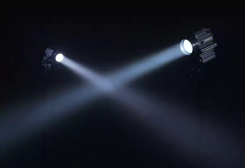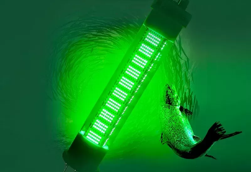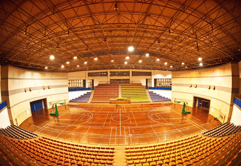
High-density solid-state lighting has transitioned decisively from distributed Surface Mount Device (SMD) topologies to concentrated Chip-on-Board (COB) architectures in high-lumen industrial and architectural applications. Within this power class, specifying an industrial-grade 200w cob led chip requires a comprehensive understanding of semiconductor packaging, thermal dynamics, and secondary optics. As luminous flux demands increase within high-bay fixtures, stadium projectors, and specialized stage lighting, system engineers must evaluate not merely the bare lumen output, but the systemic efficiency dictated by thermal interfaces, phosphor stability, and current density management.
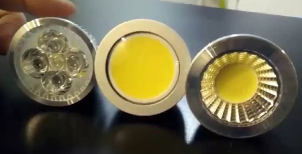
Structural Architecture and Packaging Technology
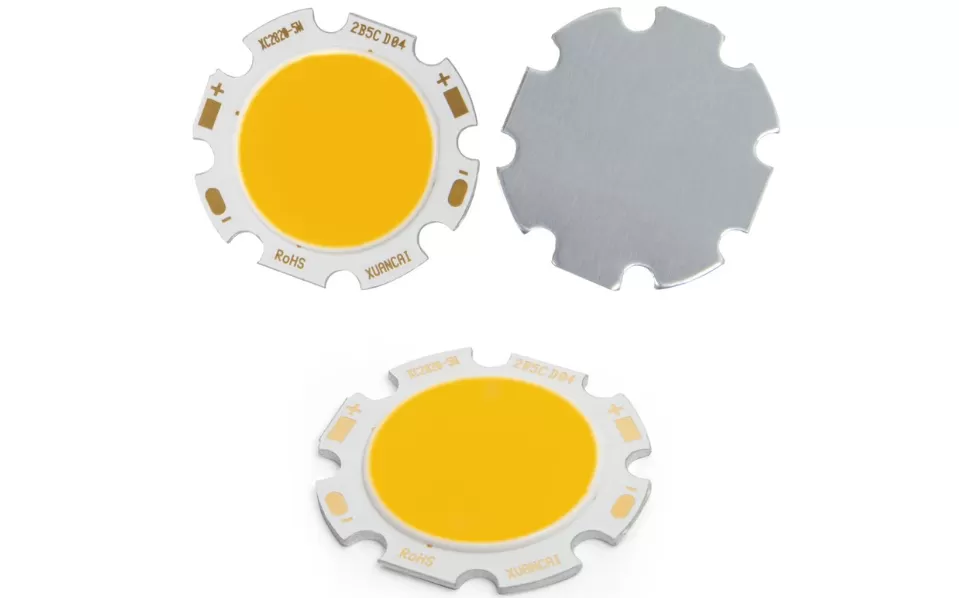
The operational lifespan and efficiency of high-wattage arrays depend heavily on the underlying materials used during packaging. When evaluating a 200w cob led chip, the structural design of the substrate dictates both thermal resistance and mechanical rigidity under cyclical thermal loads.
Substrate Metallurgy: Ceramic vs. Metal Core PCBs
Traditional lower-wattage modules frequently deploy Metal Core Printed Circuit Boards (MCPCB) utilizing an aluminum base with an epoxy dielectric layer. In 200W concentrated thermal footprints, the low thermal conductivity of organic dielectric layers (typically 1.0 to 3.0 W/mK) creates a severe thermal barrier. Industrial packaging utilizes Direct Plated Copper (DPC) or Active Metal Brazing (AMB) on ceramic substrates:
Aluminum Nitride (AlN): Offering a thermal conductivity between 170 and 220 W/mK, AlN is the preferred substrate for high-power densities. Its coefficient of thermal expansion (CTE) matches that of silicon and gallium nitride (GaN) closely, mitigating mechanical shear stress on micro-welds during rapid power cycling.
Alumina (Al2O3): While more cost-effective with a conductivity around 24 to 30 W/mK, alumina substrates demand an increased surface area, rendering them sub-optimal for fixtures requiring compact Light Emitting Surfaces (LES) for tight beam control.
Die Interconnect Strategies: Wire Bonding vs. Flip-Chip
Die-attach architecture governs electrical conduction and localized heat transfer. Wire-bonded configurations utilize gold (Au) or copper (Cu) ball bonds to connect the top-side electrodes to the circuit traces. While mature and economical, bond wires introduce structural vulnerabilities under extreme vibration and restrict heat extraction strictly through the bottom junction.
Flip-chip configurations eliminate bond wires entirely. The micro-diodes are inverted and bonded directly to the metallized ceramic substrate via gold-tin (AuSn) or lead-free solder bumps. This approach slashes thermal resistance at the chip level, eradicates wire-shadowing losses across the light output surface, and allows the package to withstand higher forward currents without bond fatigue. Advanced packaging houses such as CAS utilize high-purity aluminum nitride (AlN) direct-bonded copper substrates combined with eutectic flip-chip arrays to maximize forward drive capabilities and extend operational continuity.
Phosphor Deposition and Encapsulation Integrity
White light conversion in a high-power package places intense thermal and optical stress on the silicone-phosphor matrix. The package must dissipate not only electrical waste heat but also Stokes shift heat generated within the phosphor itself. Conventional dispensing methods can lead to uneven phosphor sedimentation, causing correlated color temperature (CCT) variations across wide viewing angles. Conformal coating and pre-formed ceramic phosphor plates guarantee uniform spectral distribution, suppressing the common problem of yellow-ring chromatic aberrations along the beam periphery.
Electro-Optical Performance Metrics
Translating power into clean, stable optical output requires precise calibration of voltage, current, and spectral quality under operating equilibrium.
Voltage and Current Operating Parameters
Operating parameters for the standard 200w cob led chip typically feature forward currents varying between 2800mA and 5400mA, depending on whether the internal array is structured in high-voltage/low-current or low-voltage/high-current matrix topologies. A standard configuration relies on a multi-series, multi-parallel (e.g., 16S12P or 12S16P) internal layout, yielding nominal forward voltages around 36V, 48V, or 54V.
Direct current ripple must be maintained below 5% to prevent micro-flicker and uneven thermal hot spots across individual die rows. Voltage binning tolerances must remain tight; mismatched forward voltages across parallel die strings promote current hogging, where a lower-resistance string draws disproportionate current, accelerating localized lumen depreciation and catastrophic string failure.
Luminous Efficacy and Spectral Optimization
Modern arrays achieve nominal cold-lumen efficiencies exceeding 160 to 180 lumens per watt (lm/W) at 25°C junction temperatures. Practical luminaire design dictates baseline testing under thermal equilibrium (junction temperature at 85°C), where real-world operational efficacy generally settles between 135 and 155 lm/W for an 80 Color Rendering Index (CRI) profile.
Balancing spectral requirements against electrical efficiency remains an engineering trade-off:
Commercial/Industrial Lighting (70–80 CRI): Maximizes lumen output per electrical watt by optimizing yellow-green phosphor components, ideal for warehouse high bays and roadway illumination.
High-Fidelity Lighting (90–97 CRI / TLCI > 95): Incorporates narrow-band red nitrides to elevate the R9 value above 50, critical for retail environments, television studios, and architectural applications. This spectral broadening typically drops absolute luminous flux by 12% to 18% compared to standard 70 CRI equivalents.
Thermal Management and Junction Temperature Engineering
Thermal dissipation represents the primary engineering bottleneck when integrating a 200w cob led chip into compact luminaires. Over 65% of the electrical energy consumed by the array is converted directly into heat rather than visible photons, concentrating up to 130W of purely conductive thermal load within an active surface area often smaller than a two-euro coin.
Mathematical Junction Calculation
The operational junction temperature determines both instantaneous photon yield and long-term lumen maintenance. The junction temperature is derived using the standard thermal resistance chain:
T_j = T_a + P_d × (R_th-jc + R_th-tim + R_th-hs)
Where:
T_j = Diode Junction Temperature (°C)
T_a = Ambient Air Temperature (°C)
P_d = Dissipated Thermal Power (W) (Total input power minus optical power emitted)
R_th-jc = Thermal resistance of the package from junction to case (°C/W)
R_th-tim = Thermal resistance of the thermal interface material (°C/W)
R_th-hs = Thermal resistance of the heatsink to ambient atmosphere (°C/W)
Maintaining a stable T_j below 85°C is targeted for standard lifespan ratings. Exceeding 105°C accelerates yellow phosphor degradation, delaminates encapsulation silicones, and drives rapid lumen loss, degrading L70 metrics from 60,000 hours down to fewer than 20,000 hours.
Heatsink Topologies: Active vs. Passive Systems
Passive cooling for a 200W concentrated source requires substantial aluminum surface area and mass, demanding fin profiles optimized for natural buoyancy-driven convective flow. Extruded, cast, or cold-forged radial pin-fin heatsinks are widely applied. For extremely compact fixture designs where physical envelope constraints prevent broad passive dissipation, phase-change solutions become practical:
Vapor Chamber Bases: Planar heat pipes embedded directly below the array rapidly spread localized flux outwards across the wider fin structure, effectively eliminating convective dead zones.
Heat Pipe Towers: Sintered copper heat pipes transfer thermal loads directly to modular exterior fins, often found in industrial stadium floodlights.
Optimizing the Thermal Interface Material (TIM)
Microscopic surface roughness between the metallic base of the ceramic substrate and the heatsink mounting face creates microscopic air voids that act as severe thermal insulators (air conductivity ~0.026 W/mK). Applying high-performance phase-change materials (PCM) or non-curing thermal greases with conductivities exceeding 4.0 to 6.0 W/mK is mandatory. Mounting torque must be calibrated precisely to achieve controlled wet-out thickness without cracking brittle ceramic substrates.
Optical System Integration and Beam Control
The optical system translates raw hemispherical lambertian emissions into controlled, task-specific photometric profiles. The physical dimensions of the Light Emitting Surface (LES) directly govern the optical properties of the luminaire.
The Role of Optical Etendue
Selecting secondary optics for a 200w cob led chip depends on the Light Emitting Surface diameter, which typically ranges from 19mm to 32mm. Etendue dictates that as the source size expands, achieving narrow beam angles (e.g., below 15 degrees) requires exponentially larger secondary reflectors or lenses.
A smaller LES delivers higher center-beam candlepower (CBCP) and enables ultra-narrow distributions suitable for architectural spot and searchlight applications. However, reducing the LES heightens optical power density, demanding superior thermal substrates to cope with the increased concentration of heat. Conversely, a wider LES eases thermal flux extraction but limits the luminaire to medium, wide, or asymmetric batwing distributions common in logistics centers.
Secondary Optical Components
System designers generally specify one of three optical solutions based on the operating environment:
Aluminum Faceted Reflectors: Vacuum-metallized aluminum reflectors offer high optical efficiencies (90-94%) and robust thermal resistance. Micro-faceting smooths localized color inconsistencies across the projected field, delivering uniform beam cutoff.
Borosilicate Glass Lenses: In high-temperature, outdoor, or chemically harsh environments, optical-grade borosilicate lenses eliminate concerns regarding UV yellowing, environmental micro-cracking, or thermal deformation that degrade polymethyl methacrylate (PMMA) or polycarbonate (PC) optics.
Total Internal Reflection (TIR) Optics: Molded optical silicone TIR collimators capture virtually all emitted photons, providing precise edge transitions and minimizing spill light in controlled architectural applications.
Power Supply Topologies and Control Architectures
Solid-state light sources are strictly current-dependent semiconductors; their longevity hinges on the electrical stability of the driving power supply. Voltage spikes, harmonic pollution, and inadequate thermal foldback within the driver rapidly impair diode lifespan.
Drivers matched with high-output arrays must maintain power factors above 0.95 and total harmonic distortion (THD) below 10% across a wide load spectrum (50% to 100% capacity). Isolated Class 1 or Class 2 power topologies must supply robust galvanic isolation to satisfy UL/CE safety directives, shielding the low-voltage package from grid fluctuations.
To assure broad luminaire adaptability, electronic drivers integrate standardized dimming interfaces:
Analog 0/1-10V Dimming: Simple and widely deployed, adjusting output linearly down to 10% or 1%, depending on the driver design.
DALI-2 Protocol: Provides bidirectional digital communication, allowing continuous operational telemetry, precise algorithmic logarithmic dimming curves, and autonomous maintenance warnings via building management systems.
Pulse-Width Modulation (PWM): Frequently utilized for stage and broadcast luminaires to maintain identical spectral CCT across dimming ranges, though high-frequency modulation (above 4 kHz) is mandatory to eliminate camera banding and stroboscopic optical artifacts.
Electronic system components certified by CAS undergo thermal shock testing
and electrical surge evaluations up to 10kV/6kA, assuring seamless
interoperability between the solid-state array and the external driver under
fluctuating power-grid conditions.
Mechanical Mounting and Automated Assembly Parameters
Assembling high-output luminaires demands high repeatability to ensure long-term mechanical contact and electrical safety.
Direct solder-lead attachments to high-wattage arrays carry liabilities: thermal expansion stresses can crack manual solder joints, while thermal transfer during hand-soldering risks damaging surrounding silicones. Luminaire manufacturers predominantly standardize on solderless mechanical holders. These holders perform multiple functions:
Apply uniform, spring-loaded mechanical pressure onto the thermal interface material without creating local stress points on the ceramic.
Integrate toolless push-in wire terminals matching standard 18-22 AWG solid or tinned-strand conductors.
Incorporate secondary optic snap-fit alignments, ensuring the optical axis of the reflector or collimator coincides precisely with the photometric center of the array.
Frequently Asked Questions
What is the typical operating lifespan of a 200W high-power COB array?
Under rated operating currents and effective thermal management where the junction temperature does not exceed 85°C, a quality module typically exhibits an L90B10 metric exceeding 50,000 hours, and an L70 lifetime beyond 75,000 hours according to IES LM-80 testing and TM-21 projection calculations.
How does LES diameter affect fixture design?
The Light Emitting Surface diameter dictates the optical punch and physical dimensions of the fixture. A smaller LES (e.g., 19mm-22mm) allows tight, narrow-beam optical control with smaller reflectors, but results in high thermal flux density. A larger LES (e.g., 28mm-32mm) spreads heat across a larger surface area, simplifying thermal management but limiting the minimum beam spread to broader distribution angles.
Why does CCT shift over time in high-output solid-state devices?
Color temperature shifting is predominantly caused by the thermal degradation of the optical silicone matrix surrounding the phosphor particles, as well as degradation of the yellow, green, or red nitrides themselves. Sustained operation at high junction temperatures alters the emission spectra of the phosphor, frequently moving the chromaticity coordinates away from the original MacAdam ellipse toward higher blue wavelengths.
What are the critical parameters when choosing a matching driver?
Key parameters include matching the driver output current window to the array's nominal drive requirements, ensuring the forward voltage range of the driver completely encompasses the operating V_f of the chip over cold-start and hot-equilibrium conditions, verifying low current ripple (<5%), and requiring integrated NTC thermal foldback protection.
Can this power class be safely dimmed to 0%?
Continuous dimming down to 0.1% or 1% is practical using contemporary digital dimming systems like DALI-2 or deep PWM. However, when employing linear analog 0-10V control, the driver typically cuts off between 5% and 10% load due to circuit thresholds. It is necessary to match the driver dimming profile to the application requirements to ensure flicker-free operation at the lower dimming limits.
Technical Inquiries and Custom Optical Solutions
Achieving peak system performance requires aligning packaging materials, thermal mechanics, optics, and electrical drivers into a balanced assembly. Engineers and luminaire manufacturers sourcing the 200w cob led chip can request tailored mechanical drawings, custom multi-spectral arrays, ray-tracing optical files (ASAP/TracePro format), and LM-80 test reports to accelerate luminaire design cycles. Submit your technical project specifications and production volume requirements directly to start a conversation with our engineering team.