Thermal dissipation remains the principal limiting factor in the pursuit of higher luminous flux densities, structural miniaturization, and decade-long operating lifespans within solid-state lighting. While organic substrates and metal-core printed circuit boards (MCPCBs) serve entry-level consumer illumination adequately, high-current injection environments require an inorganic, dimensionally stable alternative. The ceramic LED chip represents a decisive departure from legacy packaging paradigms, providing an engineered inorganic carrier that simultaneously resolves the dual challenges of heat extraction and mechanical stability.
Solid-state device engineers and optical system designers increasingly deploy ceramic substrates to handle the severe thermal gradients that occur when pushing injection currents past three to five amperes per square millimeter. By reviewing the material science, metallurgical interconnection layers, and substrate manufacturing methods that define these emitters, optical engineers can optimize their thermal architectures and achieve targeted luminous efficacy without sacrificing product longevity.
Substrate Material Sciences: Aluminum Oxide vs. Aluminum Nitride
The performance of any ceramic-packaged emitter depends fundamentally on the chemical composition and crystalline purity of the underlying dielectric base. The two dominant ceramic formulations in photonics packaging are Aluminum Oxide (Al2O3, commonly termed Alumina) and Aluminum Nitride (AlN). Each exhibits distinct thermal, mechanical, and economic tradeoffs that dictate its deployment across specific drive-current regimes.
Alumina delivers an isotropic thermal conductivity rating ranging between 20 W/m·K and 30 W/m·K. While modest compared to exotic ceramics, this baseline represents an order-of-magnitude leap over standard FR-4 laminates (approximately 0.3 to 0.8 W/m·K) and matches the volumetric thermal conductivity of standard dielectric layers used in commodity MCPCBs. Alumina features substantial mechanical hardness, dielectric breakdown strength exceeding 15 kV/mm, and favorable raw material costs. Systems running below 1.5 Watts per package typically leverage Alumina to balance manufacturing overhead with adequate heat dissipation.
Elevating drive currents into extreme flux densities shifts the mechanical requirement toward Aluminum Nitride. AlN features a theoretical bulk thermal conductivity between 170 W/m·K and 230 W/m·K, which closely approaches metallic aluminum while maintaining complete electrical isolation. Synthesized via carbothermal reduction or direct nitridation of aluminum powder, AlN demonstrates exceptional phonon-driven lattice conduction. Because heat in non-metallic solids travels via quantized lattice vibrations (phonons), the structural purity, low grain-boundary oxygen contamination, and high density of the AlN lattice yield thermal performance up to eight times greater than that of standard Alumina.
Alumina (Al2O3): 24–30 W/m·K thermal conductivity, high flexural strength, highly cost-effective for moderate power distributions.
Aluminum Nitride (AlN): 170–200+ W/m·K thermal conductivity, ideal for dense arrays, automotive matrix systems, and ultra-high-power emitters.
Silicon Nitride (Si3N4): 70–90 W/m·K thermal conductivity, outstanding fracture toughness for high cyclic thermal-shock environments.
Metallization Technologies: Direct Plated Copper vs. Direct Bonded Copper
Raw ceramic blocks are electrically inert and chemically unreactive to standard soldering alloys. Forming functional conductive paths for die attachment and electrical interconnects demands advanced substrate metallization. The packaging industry relies on Direct Plated Copper (DPC) and Direct Bonded Copper (DBC) processes to execute these high-precision traces.
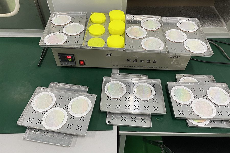
DPC utilizes physical vapor deposition (PVD) to apply an initial titanium adhesion layer, followed by a copper seed layer onto the polished ceramic surface. Photolithography creates high-resolution circuit patterns, which are then built up through electroplating to copper thicknesses between 20 and 150 microns. The DPC process provides alignment tolerances below 10 microns, near-vertical trace sidewalls, and flat surface topography. These parameters are mandatory for flip-chip placement where solder bridging between tightly pitched pads would cause catastrophic electrical shorts. Substrates produced to CAS manufacturing benchmarks routinely employ DPC architectures to preserve pad coplanarity across complex multidie configurations.
DBC attaches thick copper foil directly to the ceramic via a high-temperature eutectic melt process (typically using a Cu-Cu2O liquid phase at approximately 1065°C to 1085°C). The copper thickness on DBC substrates usually ranges from 125 to 500 microns, making them suitable for ultra-high currents exceeding tens of amperes. The geometric resolution of DBC traces remains lower than that of DPC because wet chemical etching produces lateral undercut profiles. Consequently, high-density matrix arrays favor DPC, whereas industrial power modules and monolithic heavy-die assemblies rely on the current-carrying cross-section of DBC.
Thermal Expansion Matching and Interfacial Stress Reduction
When high-brightness Gallium Nitride (GaN) or Indium Gallium Nitride (InGaN) epitaxial layers run continuously, junction temperatures (Tj) climb rapidly. The mismatch in Coefficient of Thermal Expansion (CTE) between the semiconductor die and its mounting substrate generates internal shear strain across the die-attach interface.
GaN possesses a CTE of approximately 5.6 × 10^-6 /K along the a-axis. Standard copper heat sinks exhibit an expansive CTE of 16.5 to 17.0 × 10^-6 /K, while standard structural aluminum ranges up to 23.0 × 10^-6 /K. Soldering a brittle semiconductor die directly to a copper carrier induces substantial mechanical deflection during repeated thermal cycling, culminating in micro-cracks within the active multi-quantum well (MQW) layers or delamination of the solder interface.
The ceramic LED chip neutralizes this mismatch. Alumina features a CTE between 6.8 and 8.0 × 10^-6 /K, and Aluminum Nitride provides a CTE between 4.5 and 5.3 × 10^-6 /K. By mirroring the physical expansion properties of the GaN crystal lattice, an AlN substrate eliminates high shear vectors at the joint. Utilizing Gold-Tin (AuSn) or silver sintering paste on matched ceramic carriers ensures that cyclic thermal fatigue is absorbed throughout the substrate matrix rather than shearing the delicate epitaxial layers.
Packaging Topologies: Flip-Chip Integration on Ceramic Carriers
Traditional high-power packaging routed current through microscopic gold wire bonds affixed to the top emitter surface. Wire bonds present parasitic inductance, shade the emissive aperture, and introduce a mechanical point of failure under thermal vibration. Modern high-flux applications prefer flip-chip topologies mounted directly onto metallized ceramic substrates.
In a flip-chip ceramic LED chip, the p- and n-electrodes sit on the bottom plane of the semiconductor die. The die is flipped and bonded directly to the matched DPC traces using gold-tin eutectic metallurgy or sub-micron silver sintering. Heat generated at the p-n junction escapes downward into the high-conductivity ceramic carrier without passing through sapphire or silicon substrate layers. The thermal path length shrinks to tens of microns, cutting package-level thermal resistance to under 2.0 K/W.
This layout removes optical shadowing from top-wire bonds and clears the top surface for secondary micro-optics, precise silicone moulding, or atomic-layer-deposited (ALD) phosphor coatings. Optical engineers achieve luminance densities exceeding 100 candela per square millimeter, which is essential for high-throw beam generation and compact optical assemblies.
Critical Application Environments
The mechanical and thermodynamic benefits of ceramic-based packaging translate to exceptional stability in sectors where maintenance-free duty cycles are contractually specified.
Automotive Exterior Lighting and Adaptive Driving Beams
Modern automotive headlamps demand continuous high-flux output from extremely restricted aerodynamic housings. Ambient engine-bay and localized aerodynamic temperatures routinely surpass 105°C. Ceramic devices handle these external ambient profiles without junction temperature overshoot. Adaptive driving beam (ADB) matrices, which integrate dozens of individually addressable sub-millimeter dies on a continuous AlN plane, rely on the dielectric strength and fine-line lithography of DPC ceramic technology to keep electrical cross-talk zero and thermal blooming negligible.
Industrial and High-Bay Infrastructure
In logistics centers, heavy foundries, and processing plants, luminaire replacement costs often surpass initial fixture capital expenditures. Luminaires deployed at mounting heights above 12 meters run under severe localized heat buildup beneath facility ceilings. Industrial fixtures that use ceramic packaging ensure long-term luminous maintenance, surpassing LM-80 targets by preserving the mechanical integrity of the die-attach layer across 100,000 operational hours.
Ultra-Violet and Short-Wavelength Photonic Processing
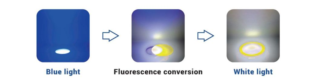
Deep-UV (UV-C, 254–280 nm) emitters constructed from Aluminum Gallium Nitride (AlGaN) experience optical-to-thermal conversion efficiencies where over 90% of supplied input power is converted immediately into heat. Organic encapsulants, standard epoxies, and polymer bases degrade and yellow rapidly under deep-UV flux. Packaging UV-C emitters with a ceramic LED chip base provides complete resistance to ultraviolet-induced polymer degradation. Gold-tin eutectic bonding directly onto AlN substrates creates an inorganic, hermetically sealable environment that withstands harsh photochemical wavelengths without structural degradation.
High-Output Horticultural Systems
Greenhouse environments expose lighting fixtures to intense humidity, elevated ambient temperatures, and corrosive airborne chemicals such as sulfur and volatilized pesticides. Ceramic carriers, sealed with inert metallization layers, resist chemical oxidation, sulfurization-induced darkening, and moisture ingress that often corrode low-cost silver-plated lead-frame packages.
Quality Specifications and Parametric Verification
Procuring and integrating ceramic emitters requires thorough validation against empirical performance parameters. Engineers must evaluate several fundamental specifications:
Thermal Resistance Junction-to-Solder Pad (Rth_j-sp): Typically dynamic between 1.5 K/W to 4.5 K/W depending on die footprint and AlN purity. Lower ratings protect internal junction stability under overdriving conditions.
Dielectric Breakdown Voltage: Premium ceramic packages provide isolation barriers exceeding 2.5 kV AC, verified through automated isolation testing, preventing substrate leakage into external structural housings.
Solder Joint Shear Strength: Shear values after reflow must exceed 30 MPa, confirming optimal metallurgical interdiffusion between the ceramic metallization and the die pads.
Die-Attach Voiding Percentage: Ultrasonic scanning acoustic microscopy (C-SAM) must verify voiding levels under 10% across the thermal pad to prevent localized hot-spotting and premature junction wear.
Phosphor-Silicone Adhesion: Inorganic packaging bases tested to CAS testing frameworks demonstrate zero border delamination under 1,000 thermal-shock cycles ranging from -40°C to 125°C.
Substrate Comparison Matrix
Engineers selecting materials for high-power illumination projects can reference the trade-offs below when sizing thermal performance against package cost:
FR-4 Glass-Reinforced Epoxy: Thermal conductivity: ~0.3 W/m·K. Die shear stability: Moderate. Dielectric strength: 15–20 kV/mm. CTE: 14–17 × 10^-6 /K. Intended application: Consumer electronics, indicator panels, low-cost general illumination.
Metal Core PCB (Aluminum MCPCB): Thermal conductivity: 1.0–3.0 W/m·K (limited by polymer dielectric layer). Die shear stability: High. Dielectric strength: 1–4 kV/mm. CTE: 18–22 × 10^-6 /K. Intended application: Medium-power LED tubes, residential downlights, standard industrial luminaires.
Alumina Ceramic (Al2O3): Thermal conductivity: 24–30 W/m·K. Die shear stability: Extremely high. Dielectric strength: 15–25 kV/mm. CTE: 6.8–8.0 × 10^-6 /K. Intended application: Mid-to-high power general luminaires, horticultural lighting, architectural spotlights.
Aluminum Nitride Ceramic (AlN): Thermal conductivity: 170–230 W/m·K. Die shear stability: Extremely high. Dielectric strength: 15–20 kV/mm. CTE: 4.5–5.3 × 10^-6 /K. Intended application: Automotive ADB, high-power stadium arrays, high-flux industrial projection, UV-C sterilization.
Frequently Asked Questions
Why does an AlN ceramic LED chip outperform an insulated metal substrate (IMS)?
An Insulated Metal Substrate relies on an organic or semi-organic dielectric layer sandwiched between the surface circuit copper and the underlying aluminum plate. This dielectric layer typically features poor thermal conductivity, ranging from 1 to 5 W/m·K, which creates a sharp thermal bottleneck. A ceramic carrier is monolithic and completely inorganic, allowing direct dissipation through its 170 to 230 W/m·K crystal lattice without an intervening organic barrier.
How does ceramic packaging eliminate the risk of sulfurization?
Standard SMD LED packages utilize silver-plated lead-frames (PPA, PCT, or EMC plastics). Airborne sulfur compounds penetrate these permeable plastic resins, reacting with the silver plate to create silver sulfide (Ag2S). This reaction blackens the internal reflector cup and cuts optical output. Ceramic packaging uses inert ceramic walls and gold-tin or nickel-gold plating that resists atmospheric sulfur ingress and chemical attack entirely.
What solder profile adjustments are required for ceramic carriers?
Ceramic packages exhibit higher thermal mass and faster heat absorption than plastic packages. Reflow soldering profiles must incorporate a extended, uniform pre-heat soak between 150°C and 180°C to prevent thermal shock, followed by a controlled ramp up to the peak reflow temperature (typically 240°C to 260°C for lead-free SAC305). Cooling rates should be managed under 3°C per second to prevent thermal-stress cracking across the ceramic body.
Can ceramic packages be driven at higher junction temperatures?
Yes. Plastic-packaged components (PPA or EMC) often restrict maximum junction temperatures to 105°C or 125°C because higher temperatures cause resin discolouration and epoxy breakdown. A ceramic LED chip easily tolerates junction temperatures up to 150°C, and specialized high-reliability variants operate reliably beyond 175°C, provided the die-attach solder and phosphor conversion layers are rated for those temperatures.
How does moisture sensitivity compare between ceramic and plastic LED packages?
Most plastic packages are rated at MSL (Moisture Sensitivity Level) 3 or 4 under JEDEC standards, absorbing atmospheric moisture that can vaporize into a "popcorn" delamination defect during high-temperature reflow. High-quality ceramic packaging achieves MSL 1 status because the substrate is non-hygroscopic and does not absorb ambient atmospheric moisture.
Engineering Consultation and Specification Request
Optical performance, thermal dissipation architectures, and spatial constraints require precise component sizing. Integrating the correct ceramic package footprint into your PCB layout eliminates performance bottlenecks before committing to tooling. Provide your target operational parameters, drive current ranges, thermal envelope constraints, and photometric objectives to the CAS optoelectronics engineering team to receive complete radiometric data sheets, thermal impedance models, and manufacturing-run quotation packages tailored directly to your system requirements.