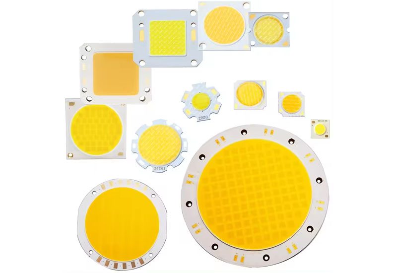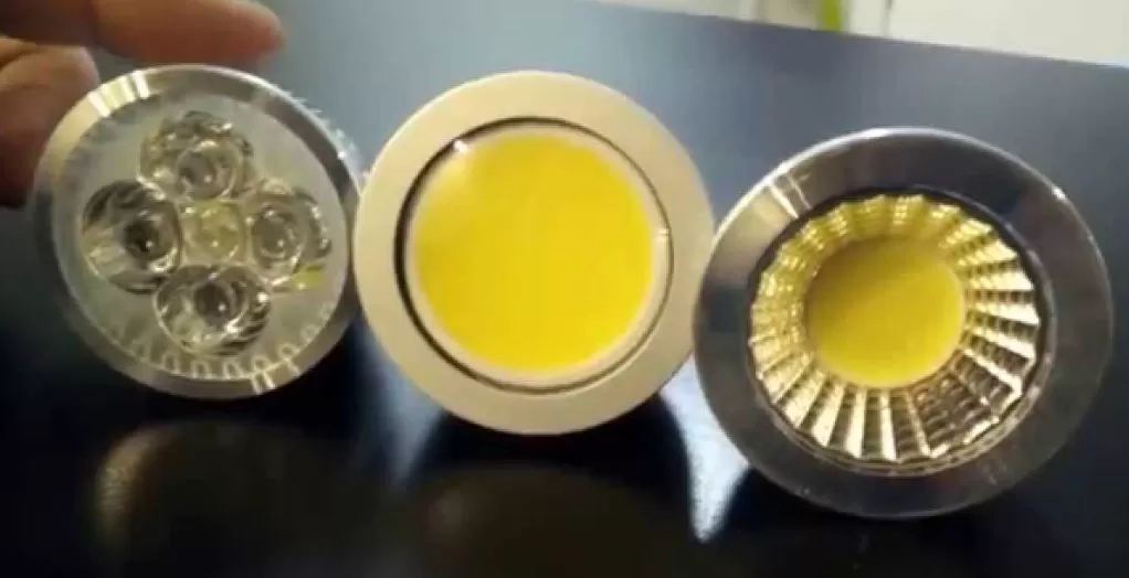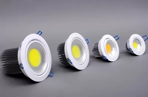
Thermal accumulation presents the single greatest obstacle to solid-state lighting performance. When driving high currents through semiconductor junctions, non-radiative recombination generates substantial heat. If this heat cannot escape quickly, radiant efficiency collapses, chromaticity shifts, and component life drops drastically.
Traditional organic plastic packages cannot handle the intense thermal loads of modern optoelectronics. As a result, the Ceramic Led Chip has become the critical hardware choice for high-power illumination. At CAS, we engineer high-performance packaging architectures designed to remove thermal bottlenecks and keep high-current emitters operating within safe junction limits.
If your project demands high lumen density, extreme reliability, and prolonged operational lifetime under harsh environments, understanding ceramic packaging is vital. Contact our engineering team today to review your project specifications or request qualification samples.
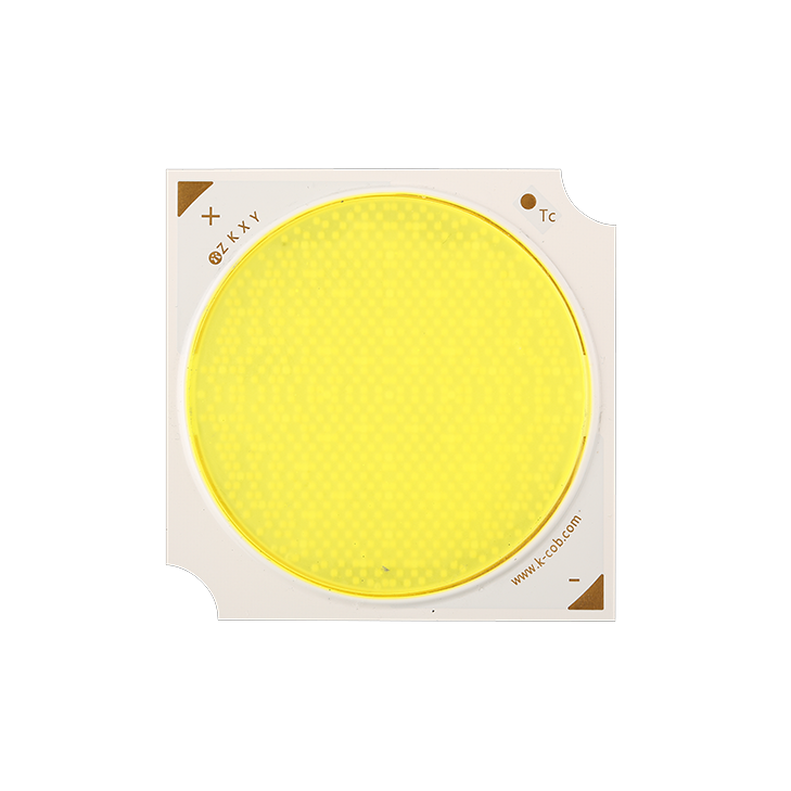
What is Ceramic LED Chip Packaging and Why Does It Matter?
A ceramic package replaces traditional plastic resin carrier structures with an inorganic, thermally conductive ceramic tile. The LED die mounts directly onto metallized circuit traces patterned onto this ceramic plate. Silicon or glass lenses sit on top, sealed with resilient optical adhesives.
Conventional Mid-Power LEDs rely on Polyphthalamide (PPA) or Epoxy Molding Compound (EMC) leadframes. These leadframes degrade rapidly when exposed to high operational temperatures and short-wavelength light. In contrast, an inorganic Ceramic Led Chip does not discolor, warp, or crack under intense photon flux or prolonged thermal stress.
Lighting systems operating past 1W per package require rapid heat extraction away from the sub-millimeter die. Research published by the U.S. Department of Energy on Solid-State Lighting highlights thermal management as the defining variable in luminaire reliability. Ceramic materials provide the required heat dissipation channels while maintaining critical electrical isolation.
| Parameter | Plastic Leadframe (PPA/EMC) | Metal Core PCB (MCPCB) | Ceramic Substrate (Al2O3 / AlN) |
|---|---|---|---|
| Thermal Conductivity (W/m·K) | 0.2 to 1.5 | 1.0 to 3.0 (dielectric layer) | 24 to 200+ |
| Operating Junction Temp (Max) | 100°C - 125°C | 120°C | 150°C - 175°C |
| Resistance to Discoloration | Low (Prone to yellowing) | N/A (Substrate level) | Immune (Inorganic matrix) |
| Package Density / Size | Bulky, low current tolerance | Medium | Ultra-compact (e.g., 3535, 2016, 1616) |
| Dielectric Breakdown Voltage | Moderate | Low to Moderate | Very High (>15 kV/mm) |
Key Substrate Materials: Al2O3 vs. AlN Ceramic LED Chips
Engineers primarily rely on two technical ceramics for solid-state packaging: Alumina (Al2O3) and Aluminum Nitride (AlN). Selecting between them dictates both thermal performance and bill-of-materials cost.
Aluminum Oxide (Al2O3)
Alumina serves as the baseline ceramic for mid-to-high wattage emitters. It provides a thermal conductivity ranging from 20 to 30 W/m·K. While modest compared to exotic ceramics, this still exceeds traditional plastics by a factor of twenty. Al2O3 offers superior mechanical rigidity and low production costs, making it a common choice for streetlights, architectural wall washers, and general outdoor luminaires.
Aluminum Nitride (AlN)
When operating currents climb past 1.5A or emitter power density exceeds 10W per square millimeter, AlN becomes essential. Aluminum Nitride yields exceptional thermal conductivity of 170 to 230 W/m·K. It dissipates concentrated heat immediately away from tiny micro-diodes, preserving internal quantum efficiency.
AlN also features a Coefficient of Thermal Expansion (CTE) between 4.3 and 4.6 × 10^-6/K. Because this closely mirrors the CTE of Gallium Nitride (GaN) and Silicon, mechanical stress during rapid thermal cycling remains minimal. This compatibility protects solder interfaces from shearing.
Advanced Packaging Technologies for Ceramic LED Chips
High thermal conductivity inside the substrate means little without robust interconnect technologies. Advanced processing techniques maximize thermal flow and mechanical strength.
- Direct Plated Copper (DPC): DPC technology combines thin-film semiconductor vacuum sputtering with copper electroplating. This creates dense, flat metallic traces on the ceramic plate without adhesive layers. The resulting surface supports fine-pitch traces and provides high peel strength.
- Flip-Chip Bonding: Traditional wire-bonded dice route electricity through fragile gold wires, which introduces thermal resistance and failure points. Modern packaging pairs the ceramic base with flip-chip architectures. The die flips upside down, placing the active P-N junction right against the copper pads.
- Eutectic Soldering: Instead of relying on thermal adhesives or silver paste, high-power assemblers use Gold-Tin (AuSn) or lead-free alloys. Eutectic bonding creates a void-free, metallic thermal path with minimal interface resistance, accelerating heat dissipation into the sub-mount.
Technical studies detailed in Electronics Cooling Magazine confirm that void-free metal interfaces lower junction-to-board thermal resistance far more effectively than standard organic glues.
Top 5 Advantages of Ceramic LED Chips in High-Power Applications
Using a Ceramic Led Chip delivers distinct structural and operational advantages over alternative packaging types.
1. Exceptional Thermal Conductivity and Low Thermal Resistance
Ceramic packaging drops junction-to-solder point thermal resistance ($R_{th, j-s}$) down to 2 to 4 °C/W. Lower thermal resistance means the junction runs cooler at equal driving currents. This increases lumens per watt and limits forward voltage drift during sustained use.
2. Precise Coefficient of Thermal Expansion (CTE) Matching
Extreme thermal cycling causes mismatched materials to expand at different rates, tearing wire bonds and cracking solder joints. Ceramic carriers match the expansion profile of sapphire and silicon dies. This stability extends product life cycles under rapid on/off switching cycles.
3. High UV Degradation Resistance
Organic silicones and plastics yellow when hit by short-wavelength ultraviolet radiation and energetic blue light. Ceramics remain completely inert to photon bombardment. Luminaire systems maintain clean lumen output and consistent correlated color temperature (CCT) over tens of thousands of hours.
4. Superior Electrical Insulation
Ceramic substrates possess innate dielectric breakdown resistance exceeding 15 kV/mm. This allows designers to route high-voltage, multi-chip arrays across a shared substrate without risking short circuits or electrical leakage to the luminaire housing.
5. High Lumen Density and Miniaturization
Because ceramics transfer heat so quickly, lighting manufacturers can place multiple high-power dies extremely close together. This footprint compression simplifies optical design. Smaller, high-precision lenses deliver narrow, punchy beam profiles without light scattering.
Real-World Applications: Where Ceramic LED Chips Dominate
Harsh operating conditions demand robust packaging solutions. The following industries depend heavily on the mechanical and thermal integrity of ceramic-based devices.
Automotive Exterior Lighting
Modern vehicle headlamps, daytime running lights, and Adaptive Driving Beam (ADB) systems operate inside hot, unventilated engine enclosures. Automotive forward lighting requires pin-point luminance to focus beam paths hundreds of meters down the road. Automotive-grade packaging manufactured by CAS delivers the intense drive-current capacity and AEC-Q102 reliability standards required by tier-1 automotive suppliers.
Mobile Device Flash Units
Smartphone flash modules demand maximum optical burst power from an ultra-thin footprint (under 2.0 × 1.6 mm). Using a micro-scale Ceramic Led Chip with a direct-eutectic flip-chip interface allows camera flashes to produce several hundred lumens for short exposures without burning the sub-mount.
Specialty Industrial and Entertainment Lighting
Stadium floodlights, high-bay factory lights, and concert moving-head fixtures pull massive continuous power. These fixtures run at high ambient temperatures for hours at a time. Ceramic emitters maintain structural stability under these loads, meeting stringent L70/B50 lifetime targets.
UV-A and UV-C Disinfection
Ultraviolet LEDs degrade organic polymers within hours of activation. As a result, UV-C solid-state chips exclusively employ AlN ceramic sub-mounts combined with direct gold-tin eutectic bonding and quartz windows. The IEEE Electron Devices Society documents significant life-cycle extensions when moving UV emitters from organic frames to ceramic carriers.
Future Trends in Ceramic LED Packaging
Packaging technology continues to evolve alongside demands for smaller footprints and lower system costs. One prominent trend involves integrating passive components directly into the ceramic base. Multi-layer High Temperature Co-fired Ceramic (HTCC) and Low Temperature Co-fired Ceramic (LTCC) designs now embed Transient Voltage Suppression (TVS) diodes and thermal sensors beneath the circuit layer.
Mini and Micro-LED displays also benefit from ceramic technology. As pitch distances shrink below 0.5 mm, organic boards suffer from structural warpage and localized heat spots. Ultra-thin, laser-machined ceramic carriers offer the flat, thermally stable platform required for high-yield micro-die transfer printing.
Frequently Asked Questions (FAQs)
Q1: How does a Ceramic LED Chip compare to an EMC LED chip in total
project cost?
A1: A Ceramic Led Chip carries a
higher initial unit cost than an Epoxy Molding Compound (EMC) package. However,
the ceramic device handles significantly higher drive currents without
overheating. This enables lighting engineers to replace multiple mid-power
plastic LEDs with fewer high-power ceramic emitters. Using fewer emitters
simplifies optical design, reduces board dimensions, shrinks the secondary heat
sink, and ultimately lowers the overall system bill-of-materials.
Q2: What is the typical thermal resistance of a ceramic packaging
sub-mount?
A2: Ceramic packages built on direct-plated copper with
Aluminum Nitride substrates generally exhibit thermal resistance figures between
1.5°C/W and 4.0°C/W. By comparison, conventional plastic packages display
thermal resistance values ranging from 10°C/W to well over 30°C/W, depending on
leadframe construction.
Q3: Can ceramic LEDs replace Chip-on-Board (COB) modules in high-bay
fixtures?
A3: Yes. High-density arrays built using discrete ceramic
emitters provide superior optical control compared to large COB modules.
Individual ceramic units produce narrow optical angles using compact secondary
lenses. This minimizes beam spill, improves target illuminance, and simplifies
field servicing compared to single-source high-wattage COB modules.
Q4: Why does a Ceramic LED Chip withstand UV light better than a
silicone-molded plastic chip?
A4: UV radiation breaks carbon-carbon
and carbon-hydrogen bonds within organic plastics, triggering yellowing,
micro-cracking, and mechanical breakdown. Technical ceramics consist entirely of
inorganic ionic and covalent crystalline lattices. High-energy ultraviolet
photons cannot break these mineral matrices, ensuring the sub-mount maintains
structural integrity.
Q5: What soldering methods work best for surface-mounting high-power
ceramic emitters?
A5: Reflow soldering using SAC305
(Tin-Silver-Copper) or low-voiding solder paste produces the best results.
Fabricators must follow strict thermal ramp profiles to avoid thermal shock to
the ceramic matrix. Establishing a void rate under 15% underneath the central
thermal pad is critical to maintaining low heat-transfer resistance.
Optimize Your Next High-Power Lighting System
Selecting the right packaging architecture determines whether an illumination system succeeds in the field or fails from premature output decay. A well-designed Ceramic Led Chip provides the thermal path, structural rigidity, and material stability required to push optical output to its physical limits.
CAS supplies custom, precision-engineered ceramic optoelectronic solutions for critical industrial, architectural, and automotive applications. Our packaging line covers high-conductivity Al2O3 tiles and AlN DPC carriers tailored to challenging operating conditions. Submit an inquiry to our sales engineering desk today to review thermal calculations, discuss circuit layouts, or request an evaluation kit for your development team.