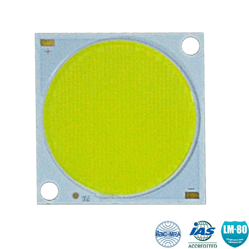
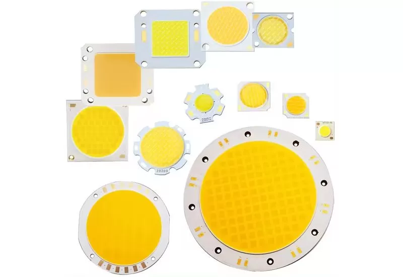
Cob surface light source
COB surface light source is the on-board chip packaging, which is one of the bare chip mounting technologies. The semiconductor chip handover is mounted on the PRINTED circuit board, and the electrical connection between the chip and the substrate is realized by lead suture method, and covered with resin to ensure reliability. Although COB is the simplest bare-chip mount technology, its package density is nowhere near as high as TAB and reverse chip welding. Therefore, the COB plane light source through the COB package form is also called COB light source,COB plane light source,COB integrated light source, ceramic COB light source

Packaging technology
1. Clean the PCB
After cleaning, the PCB board still has oil or oxide layer and other unclean parts. Use skin wipe test help to locate or test needle position. Wipe the PCB board with a brush or blow clean before flowing into the next process. For anti-static strict products to use ion dust blower. The purpose of cleaning is to clean the dust and oil stains on the PCB board bonding pad to improve the quality of bonding.

2. Drip adhesive glue
The purpose of drop adhesive is to prevent the product from dying off during transmission and bonding. Needle transfer and pressure injection are commonly used in the COB process. Needle transfer: A small drop of adhesive point is taken from the container with a needle and applied to the PCB. Put the glue into the syringe and apply a certain air pressure to extrude the glue. The size of the glue point is determined by the diameter of the syringe nozzle and the pressure time and pressure, and is related to the viscosity. The size and height of the drops are determined by the type of DIE chip (DIE), size, distance from PAD bit, and weight. The size and weight of the chip glue drop is large, it should not be too large to ensure enough viscosity shall be subject to, at the same time the adhesive can not pollute the state line pad. If must say to have the word of what standard, that also can press different product to decide only. Hard what can not exceed the chip 1/3 height can not dew glue as a standard, there is no need for this.
3. Chip paste
Chip paste is also called DIE BOND (solid crystal) stick DIE bon DIE BON IC and other companies called different. In the chip paste, vacuum suction pen (nozzle) material hardness should be small (also some companies use cotton stick). Nozzle diameter depends on chip size, tip must be flat to avoid scratching DIE surface. When pasting, check the DIE and PCB model, and check whether the pasting direction is correct. DIE towel to PCB must be “smooth”, “flat” means DIE and PCB are parallel to close without virtual position, “stable” means DIE and PCB are not easy to fall off in the whole process, “positive” means DIE and PCB are properly attached to the reserved position, and cannot be twisted. It must be noted that the chip (DIE) direction should not be reversed.

4. Bond wire (lead bonding)
Bond (lead BONDING) Wire Bond is called different here take Bond as an example Bond Bond according to the position of the BONDING diagram to connect the two solder joints of each Bond, so that it can reach the electrical and mechanical connection. PCB of Bonding is required to conform to the standard of the company when conducting bonding tension test (refer to 1.0 wire greater than or equal to 3.5g and 1.25 wire greater than or equal to 4.5g). Aluminum wire solder joint shape is oval, gold wire solder joint shape is spherical. Standard aluminum wire with fixed melting point: The length of the solder joint is greater than or equal to 1.5 times the wire diameter is less than or equal to 5.0 times the wire diameter. The width of the solder joint is greater than or equal to 1.2 times the wire diameter is less than or equal to 3.0 times the wire diameter The height of the arc is equal to the parabolic height of the circle (not too high, not too low, depending on the product) The welding ball generally online diameter of about 2.6-2.7 times in the process of the state line should be taken lightly, to the point to be accurate, operating personnel to observe the process of the state line with a microscope, to see whether there is a broken line, coil, deviation, hot and cold welding, aluminum, such as bad phenomenon, if there is immediate notice management workers or technical personnel. Before the formal production, there must be a special person for the first inspection, check whether the state is wrong, less state, state tension and so on. There should be a special person to check its correctness every 2 hours.
")
5. Sealant
Sealing glue is mainly to test OK PCB board for black glue. When dispensing, attention should be paid to the black glue should completely cover the PCB solar circle and the aluminum wire of the bonding chip, no Ruth phenomenon, the black glue should not be sealed outside the solar circle and other places of the black glue, such as glue leakage with cloth immediately wipe off. The needle tip or the tip should not touch the DIE and the bonded thread during the whole process of glue dropping. After drying, there shall be no pores on the surface of the vinyl, and the vinyl is not cured. The height of black glue is not more than 1.8mm, and the temperature of preheating plate and drying temperature should be strictly controlled when dispensing should be less than 1.5mm. Vibration its BE-08 vinyl FR4PCB board for example: (preheating temperature 120±15 degrees time 1.5-3.0 minutes drying temperature 140±15 degrees time 40-60 minutes) glue sealing method is usually also used needle transfer method and pressure injection method. Some companies also use glue drip machine, but its cost is low efficiency. Usually cotton swabs and syringes are used to drop glue, but the operator should have skilled operation ability and strict technological requirements. If you break the chip, it’s very difficult to repair it. Therefore, this process management personnel and engineering personnel must be strictly controlled.
6. Test
Because there will be some bad phenomena in the process of bonding, such as wire breaking, wire winding, fake welding and so on, which will lead to chip failure, so the chip level packaging should be tested.

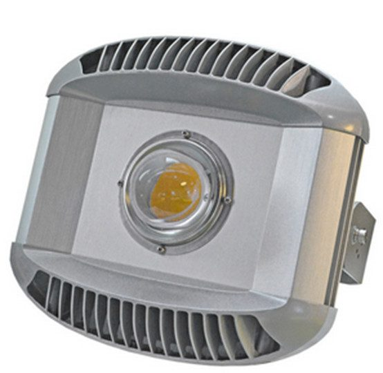
In summary, chip-on-board LEDs are the latest and most advanced technology on the market today. Simply put, COB LEDs are brighter, consume less power, and output a higher quality beam of light compared to older LED technologies found in most other trade show lighting today. The next time you are in the market for exhibit lighting, insist on COB LED technology!